
Table 1.3.2. Definition of hexadecimal representation.
For example, the hexadecimal number for the 16-bit binary 0001 0010 1010 1101 is
0x12AD = 1 • 16 3 + 2 • 16 2 + 10 • 16 1 + 13 • 16 0 = 4096+512+160+13 = 4781
Interactive Tool 1.2
You have already learned how to convert from a hexadecimal number to its decimal representation. All you need to do is to calculate its value by multiplying each coefficient by its placeholder values and summing all of them together. If you want to practice, Choose an 4-digit hexadecimal number number. Try to calculate the decimal representation. Then type the number in the following field and click "convert" to check your result.
Checkpoint 1.3.2 : What is the numerical value of the 8-bit hexadecimal number 0xFF?
Checkpoint 1.3.3 : Convert the binary number 01000101 2 to hexadecimal.
Checkpoint 1.3.4 : Convert the binary number 110010101011 2 to hexadecimal.
Checkpoint 1.3.5 : Convert the hex number 0x40 to binary.
Checkpoint 1.3.6 : Convert the hex number 0x63F to binary.
Checkpoint 1.3.7 : How many binary bits does it take to represent 0x123456?
Precision is the number of distinct or different values. We express precision in alternatives, decimal digits, bytes, or binary bits. Alternatives are defined as the total number of possibilities. For example, an 8-bit number format can represent 256 different numbers. An 8-bit digital to analog converter (DAC) can generate 256 different analog outputs. An 8-bit analog to digital converter (ADC) can measure 256 different analog inputs. Table 1.3.3 illustrates the relationship between precision in binary bits and precision in alternatives. The operation [[ x ]] is defined as the greatest integer of x . E.g., [[2.1]] [[2.9]] and [[3.0]] are all equal to 3. The Bytes column in Table 2.1 specifies how many bytes of memory it would take to store a number with that precision assuming the data were not packed or compressed in any way.
Binary bits
Alternatives
Table 1.3.3. Relationship between bits, bytes and alternatives as units of precision.
Checkpoint 1.3.8 : How many bytes of memory would it take to store a 50-bit number?
A byte contains 8 bits as shown in Figure 1.3.1, where each bit b 7 . b 0 is binary and has the value 1 or 0. We specify b 7 as the most significant bit or MSB, and b 0 as the least significant bit or LSB.

Figure 1.3.1. 8-bit binary format.
If a byte is used to represent an unsigned number, then the value of the number is
Notice that the significance of bit n is 2 n . There are 256 different unsigned 8-bit numbers. The smallest unsigned 8-bit number is 0 and the largest is 255. For example, 00001010 2 is 8+2 or 10. The least significant bit can tell us if the number is even or odd.
Checkpoint 1.3.9 : Convert the binary number 01101001 2 to unsigned decimal.
Checkpoint 1.3.10 : Convert the hex number 0x54 to unsigned decimal.
The basis of a number system is a subset from which linear combinations of the basis elements can be used to construct the entire set. The basis represents the “places” in a “place-value” system. For positive integers, the basis is the infinite set , and the “values” can range from 0 to 9. Each positive integer has a unique set of values such that the dot-product of the value vector times the basis vector yields that number. For example, 2345 is (…, 2,3,4,5) · (…, 1000,100,10,1), which is 2*1000+3*100+4*10+5. For the unsigned 8-bit number system, the basis elements are
The values of a binary number system can only be 0 or 1. Even so, each 8-bit unsigned integer has a unique set of values such that the dot-product of the values times the basis yields that number. For example, 69 is (0,1,0,0,0,1,0,1) · (128,64,32,16,8,4,2,1), which equals 0*128+1*64+0*32+0*16+0*8+1*4+0*2+1*1. Conveniently, there is no other set of 0’s and 1’s, such that set of values multiplied by the basis is 69. In other words, each 8-bit unsigned binary representation of the values 0 to 255 is unique.
One way for us to convert a decimal number into binary is to use the basis elements. The overall approach is to start with the largest basis element and work towards the smallest. More precisely, we start with the most significant bit and work towards the least significant bit. One by one, we ask ourselves whether or not we need that basis element to create our number. If we do, then we set the corresponding bit in our binary result and subtract the basis element from our number. If we do not need it, then we clear the corresponding bit in our binary result. We will work through the algorithm with the example of converting 100 to 8-bit binary, see Table 2.4. We start with the largest basis element (in this case 128) and ask whether or not we need to include it to make 100? Since our number is less than 128, we do not need it, so bit 7 is zero. We go the next largest basis element, 64 and ask, “do we need it?” We do need 64 to generate our 100, so bit 6 is one and we subtract 100 minus 64 to get 36. Next, we go the next basis element, 32 and ask, “do we need it?” Again, we do need 32 to generate our 36, so bit 5 is one and we subtract 36 minus 32 to get 4. Continuing along, we do not need basis elements 16 or 8, but we do need basis element 4. Once we subtract the 4, our working result is zero, so basis elements 2 and 1 are not needed. Putting it together, we get 01100100 2 (which means 64+32+4).
Checkpoint 1.3.11 : In this conversion algorithm, how can we tell if a basis element is needed?
Observation: If the least significant binary bit is zero, then the number is even.
Observation: If the right-most n bits (least sign.) are zero, then the number is divisible by 2 n .
Observation: Consider an 8-bit unsigned number system. If bit 7 is low, then the number is between 0 and 127, and if bit 7 is high then the number is between 128 and 255.
Checkpoint 1.3.12 : Give the representations of the decimal 45 in 8-bit binary and hexadecimal.
Checkpoint 1.3.13 : Give the representations of the decimal 200 in 8-bit binary and hexadecimal.
Interactive Tool 1.3
There are a few techniques for converting decimal numbers to binaries. One of them is consecutive divisions. We start by dividing the decimal number by 2. Then we iteratively divide the result (the quotient) by 2 until the answer is 0. The equivalent binary is formed by the remainders of the divisions. The last remainder found is the most significant digit. Enter a number between 0 and 255 in the following field and click convert to see an example. Try to convert a decimal number to binary.
One of the first schemes to represent signed numbers was called one’s complement. It was called one’s complement because to negate a number, we complement (logical not) each bit. For example, if 25 equals 00011001 2 in binary, then –25 is 11100110 2 . An 8-bit one’s complement number can vary from ‑127 to +127. The most significant bit is a sign bit, which is 1 if and only if the number is negative. The difficulty with this format is that there are two zeros +0 is 00000000 2 , and –0 is 11111111 2 . Another problem is that one’s complement numbers do not have basis elements. These limitations led to the use of two’s complement.
The two’s complement number system is the most common approach used to define signed numbers. It is called two’s complement because to negate a number, we complement each bit (like one’s complement), then add 1. For example, if 25 equals 00011001 2 in binary, then –25 is 11100111 2 . If a byte is used to represent a signed two’s complement number, then the value of the number is
Observation: One usually means two’s complement when one refers to signed integers.
There are 256 different signed 8-bit numbers. The smallest signed 8-bit number is -128 and the largest is 127. For example, 10000010 2 equals -128+2 or -126.
Checkpoint 1.3.14 : Convert the signed binary number 11011010 2 to signed decimal.
Checkpoint 1.3.15 : Are the signed and unsigned decimal representations of the 8-bit hex number 0x95 the same or different?
For the signed 8-bit number system the basis elements are
Observation: The most significant bit in a two’s complement signed number will specify the sign.
Notice that the same binary pattern of 11111111 2 could represent either 255 or –1. It is very important for the software developer to keep track of the number format. The computer cannot determine whether the 8‑bit number is signed or unsigned. You, as the programmer, will determine whether the number is signed or unsigned by the specific assembly instructions you select to operate on the number. Some operations like addition, subtraction, and shift left (multiply by 2) use the same hardware (instructions) for both unsigned and signed operations. On the other hand, divide, and shift right (divide by 2) require separate hardware (instruction) for unsigned and signed operations.
Observation: To take the negative of a two’s complement signed number we first complement (flip) all the bits, then add 1.
A second way to convert negative numbers into binary is to first convert them into unsigned binary, then do a two’s complement negate. For example, we earlier found that +100 is 01100100 2 . The two’s complement negate is a two-step process. First we do a logic complement (flip all bits) to get 10011011 2 . Then add one to the result to get 10011100 2 .
Checkpoint 1.3.16 : Give the representations of -54 in 8-bit binary and hexadecimal.
Checkpoint 1.3.17 : Why can’t you represent the number 150 using 8-bit signed binary?
When dealing with numbers on the computer, it will be convenient to memorize some Powers of 2 as shown in Table 1.3.4.
1024 about a thousand
about a million
about a billion
about a trillion
Table 1.3.4. Some powers of two that will be useful to memorize.
Checkpoint 1.3.18 : Use Table 1.3.4 to determine the approximate value of 2 32 ?
A halfword or double byte contains 16 bits, where each bit b 15 . b 0 is binary and has the value 1 or 0, as shown in Figure 1.3.2.
Figure 1.3.2. 16-bit binary format.
If a halfword is used to represent an unsigned number, then the value of the number is
N = 32768 • b 15 + 16384 • b 14 + 8192 • b 13 + 4096 • b 12
+ 2048 • b 11 + 1024 • b 10 + 512 • b 9 + 256 • b 8
There are 65536 different unsigned 16-bit numbers. The smallest unsigned 16-bit number is 0 and the largest is 65535. For example, 0010000110000100 2 or 0x2184 is 8192+256+128+4 or 8580.
Checkpoint 1.3.19 : Convert the 16-bit binary number 0010000001101010 2 to unsigned decimal.
Checkpoint 1.3.20 : Convert the 16-bit hex number 0x1234 to unsigned decimal.
For the unsigned 16-bit number system the basis elements are
Checkpoint 1.3.21 : Convert the unsigned decimal number 1234 to 16-bit hexadecimal.
Checkpoint 1.3.22 : Convert the unsigned decimal number 10000 to 16-bit binary.
There are also 65536 different signed 16-bit numbers. The smallest two’s complement signed 16‑bit number is –32768 and the largest is 32767. For example, 1101000000000100 2 or 0xD004 is –32768+16384+4096+4 or –12284.
If a halfword is used to represent a signed two’s complement number, then the value of the number is
N = -32768 • b 15 + 16384 • b 14 + 8192 • b 13 + 4096 • b 12
+ 2048 • b 11 + 1024 • b 10 + 512 • b 9 + 256 • b 8
Checkpoint 1.3.23 : Convert the 16-bit hex number 0x1234 to signed decimal.
Checkpoint 1.3.24 : Convert the 16-bit hex number 0xABCD to signed decimal.
For the signed 16-bit number system the basis elements are
Common Error: An error will occur if you use 16-bit operations on 8-bit numbers, or use 8-bit operations on 16-bit numbers.
Maintenance Tip: To improve the clarity of your software, always specify the precision of your data when defining or accessing the data.
Checkpoint 1.3.25 : Convert the signed decimal number 1234 to 16-bit hexadecimal.
Checkpoint 1.3.26 : Convert the signed decimal number –10000 to 16-bit binary.
A word on the ARM Cortex M will have 32 bits. Consider an unsigned number with 32 bits, where each bit b 31 . b 0 is binary and has the value 1 or 0. If a 32-bit number is used to represent an unsigned integer, then the value of the number is
N = 2 31 • b31 + 2 30 • b30 + . + 2 • b1 + b0 = sum( 2 i • bi ) for i=0 to 31
There are 2 32 different unsigned 32-bit numbers. The smallest unsigned 32-bit number is 0 and the largest is 2 32 -1 (4,294,967,295). This range is 0 to about 4 billion. For the unsigned 32-bit number system, the basis elements are
If a 32-bit binary number is used to represent a signed two’s complement number, then the value of the number is
N = -2 31 • b31 + 2 30 • b30 + . + 2 • b1 + b0 = -2 31 • b31 + sum( 2 i • bi ) for i=0 to 30
There are also 2 32 different signed 32-bit numbers. The smallest signed 32-bit number is -2 31 (-2,147,483,648) and the largest is 2 31 -1 (+2,147,483,647). This range is about -2 billion to about +2 billion. For the signed 32-bit number system, the basis elements are
Interactive Tool 1.4
The computer does not distinguish between signed and unsigned numbers in memory. The interpretation is yours to make. Enter an 8-bit binary number in the following field and press "show" to see its value if interpreted as signed or unsigned integer. For convenience, you can also enter hexadecimal input with '0x' prefix.
A computer combines a processor, random access memory (RAM), read only memory (ROM), and input/output (I/O) ports. Computers are not intelligent. Rather, you are the true genius. Computers are electronic idiots. They can store a lot of data, but they will only do exactly what we tell them to do. Fortunately, however, they can execute our programs quite quickly, and they don’t get bored doing the same tasks over and over again. Software is an ordered sequence of very specific instructions that are stored in memory, defining exactly what and when certain tasks are to be performed. It is a set of instructions, stored in memory, that are executed in a complicated but well-defined manner. The processor executes the software by retrieving and interpreting these instructions one at a time. A microprocessor is a small processor, where small refers to size (i.e., it fits in your hand) and not computational ability.
A microcomputer is a small computer, where again small refers to size (i.e., you can carry it) and not computational ability. For example, a desktop PC is a microcomputer. Small in this context describes its size not its computing power. Consequently, there can be great confusion over the term microcomputer, because it can refer to a very wide range of devices from a PIC12C508, which is an 8-pin chip with 512 words of ROM and 25 bytes RAM, to the most powerful I7-based personal computer.
A pin is a signal or wire on the microcomputer. Figure 1.4.1 shows MSPM0G3507 has 64 pins. A port is a collection of pins, providing a physical connection between the computer and its outside world. Ports allow information to enter and exit the system. Information enters via the input ports and exits via the output ports. Other names used to describe ports are I/O ports, I/O devices, interfaces, or sometimes just devices. A bus is a collection of wires used to pass information between modules.
A very small microcomputer, called a microcontroller, contains all the components of a computer (processor, memory, I/O) on a single chip. As shown in Figure 1.4.1, the Atmel ATtiny, the Texas Instruments MSP430, and the Texas Instruments MSPM0G3507 are examples of microcontrollers. Because a microcomputer is a small computer, this term can be confusing because it is used to describe a wide range of systems from a 6-pin ATtiny4 running at 1 MHz with 512 bytes of program memory to a personal computer with state-of-the-art 64-bit multi-core processor running at multi-GHz speeds having terabytes of storage.
The computer can store information in RAM by writing to it, or it can retrieve previously stored data by reading from it. RAMs are volatile; meaning if power is interrupted and restored the information in the RAM is lost.
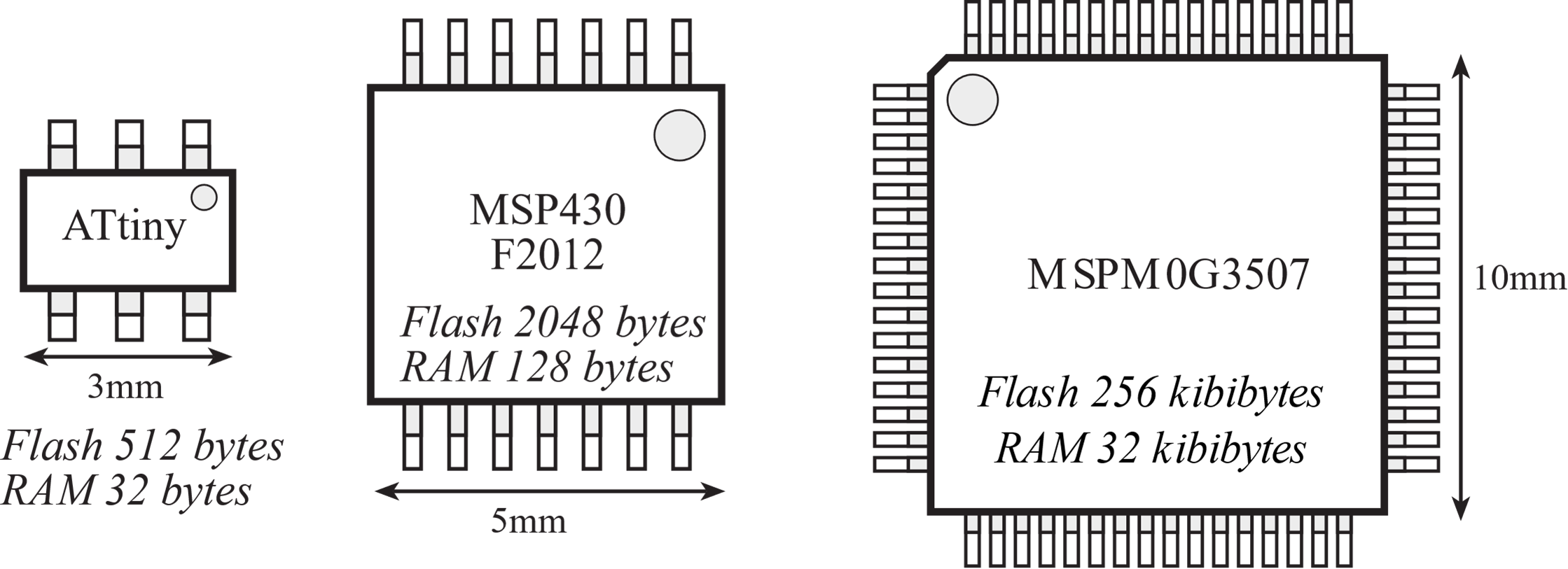
Figure 1.4.1. A microcontroller is a complete computer on a single chip.
Information is programmed into ROM using techniques more complicated than writing to RAM. From a programming viewpoint, retrieving data from a ROM is identical to retrieving data from RAM. ROMs are nonvolatile; meaning if power is interrupted and restored the information in the ROM is retained.
Figure 1.4.2 shows a simplified block diagram of a microcontroller based on the ARM ® Cortex ™ -M4 processor. It is a Harvard architecture because it has separate data and instruction buses. Instructions are fetched from flash ROM using the ICode bus at the same time as Data are exchanged with memory and I/O via the System bus interface.
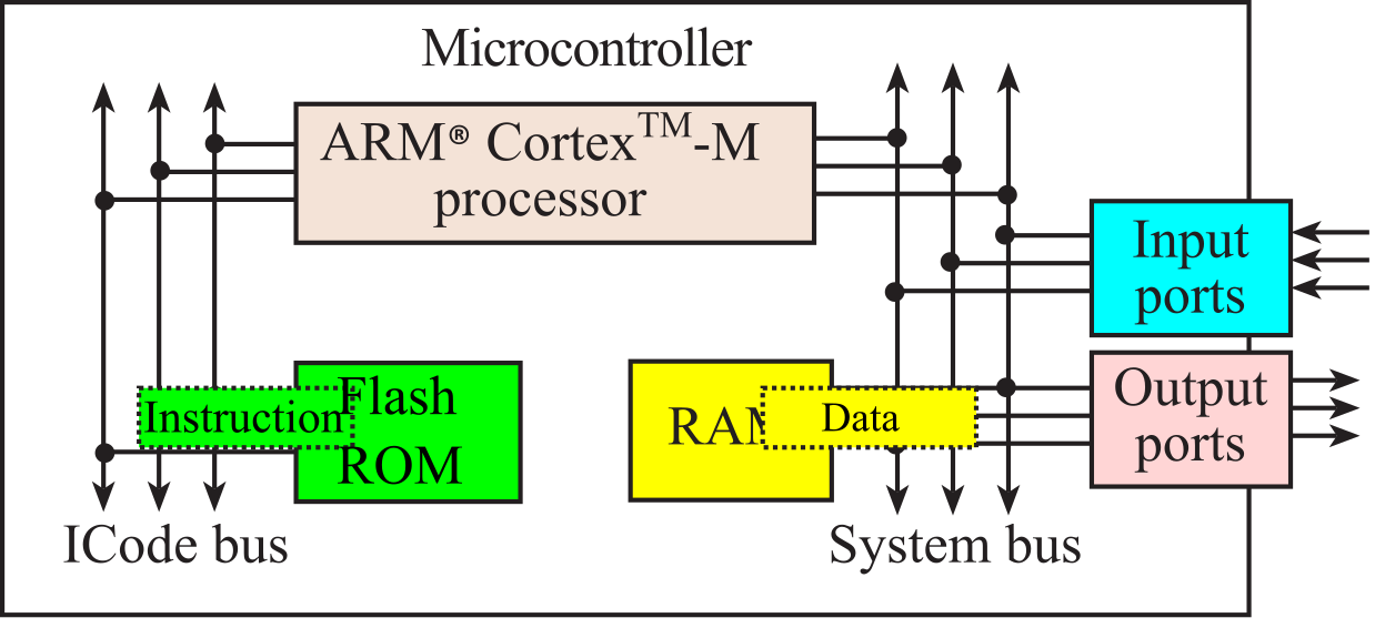
Figure 1.4.2. Harvard architecture of an ARM ® Cortex-M4-based microcontroller. Notice multiple buses allow simultaneous data flow.
The common bus in Figure 1.4.3 defines the von Neumann architecture, because a single bus is used for both data and instructions.

Figure 1.4.3. von Neumann architecture of an ARM ® Cortex-M0-based microcontroller. Notice the single bus requires data to flow one at a time.
Checkpoint 1.4.1 : What are the differences between a microcomputer, a microprocessor, and a microcontroller?
Checkpoint 1.4.2 : What are three differences between RAM and ROM?
Checkpoint 1.4.3 : What is the difference between Harvard and von Neumann architectures?
Figure 1.5.1 shows the memory map of the MSPM0G3507. A 32-bit entry requires four sequential locations. The I/O ports exist as memory-mapped locations. I/O ports are not memory, but we will write to an I/O port address to output and read from an I/O port address to input.
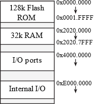
Figure 1.5.1. Memory map. Each address contains 8 bits or 1 byte.
When we store 16-bit data into memory it requires two bytes. Since the memory systems on most computers are byte addressable (a unique address for each byte), there are two possible ways to store in memory the two bytes that constitute the 16-bit data. Many main-frame computers, like the z/Architecture, implement the big endian approach that stores the most significant byte at the lower address. Most smaller computers (desktops, laptops, phones and microcontrollers) implement the little endian approach that stores the least significant byte at the lower address. The Cortex-M microcontrollers use the little endian format. Many ARM processors are biendian, because they can be configured to efficiently handle both big and little endian data. Instruction fetches on the ARM are always little endian. Figure 1.5.2 shows two ways to store the 16-bit number 1000 (0x03E8) at locations 0x20200850 and 0x20200851. We also could use either the big or little endian approach when storing 32-bit numbers into memory that is byte (8-bit) addressable. Figure 1.5.3 shows the big and little endian formats that could be used to store the 32-bit number 0x12345678 at locations 0x20200850 through 0x20200853.

Figure 1.5.2. Example of big and little endian formats of a 16-bit number (the Cortex M used little endian).

Figure 1.5.3. Example of big and little endian formats of a 32-bit number (the Cortex M used little endian).
In the previous two examples, we normally would not pick out individual bytes (e.g., the 0x12), but rather capture the entire multiple byte data as one nondivisable piece of information. On the other hand, if each byte in a multiple byte data structure is individually addressable, then both the big and little endian schemes store the data in first to last sequence. For example, if we wish to store the four ASCII characters ‘LM3S’, which is 0x4C4D3353 at locations 0x20200850 through 0x20200853, then the ASCII ‘L’=0x4C comes first in both big and little endian schemes, as illustrated in Figure 1.5.4.
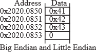
Figure 1.5.4. Character strings are stored in the same for both big and little endian formats.
The terms “big and little endian” come from Jonathan Swift’s satire Gulliver’s Travels. In Swift’s book, a Big Endian refers to a person who cracks their egg on the big end. The Lilliputians were Little Endians because they insisted that the only proper way is to break an egg on the little end. The Lilliputians considered the Big Endians as inferiors. The Big and Little Endians fought a long and senseless war over the best way to crack an egg.
Common Error: An error will occur when data is stored in Big Endian by one computer and read in Little Endian format on another.
Checkpoint 1.5.1 : Consider memory shown in Figure 1.5.4. What would you get if you did an 8-bit read from location 0x2020.0850?
Checkpoint 1.5.2 : Consider memory shown in Figure 1.5.4. What would you get if you did a 16-bit read from location 0x2020.0850?
Checkpoint 1.5.3 : Consider memory shown in Figure 1.5.4. What would you get if you did a 32-bit read from location 0x2020.0850?
A pseudo-op is an assembler directive to affect the assembly process. We use the .data pseudo-op to specify what information goes in RAM and the .text pseudo-op to specify what information what goes in ROM. We will use a template similar to Program 1.6.1 for most assembly programs in this class. The .equ pseudo-ops create symbols containing the address of some the I/O port registers. The .data pseudo-op means the subsequent code will be placed in volatile RAM. The .align 2 pseudo-op skips 0-3 bytes so the address of next object is word aligned (bottom two bits of the address are 0). The .space pseudo-op allocates 4 bytes (in RAM) for the variable named Stuff. The .text pseudo-op means the subsequent code will be placed in nonvolatile ROM. The .thumb pseudo-op tells the assembler to create Thumb code. The .global pseudo-op allows the label main to be accessed from another file. In particular, main will be the place the software starts on power up or on reset. The B Loop instruction creates an infinite loop, typical of embedded systems, causing the code between Loop and B Loop to be executed over and over.
.equ GPIOA_DOE31_0, 0x400A12C0
.equ GPIOA_DOUT31_0, 0x400A1280
.equ GPIOA_DIN31_0, 0x400A1380
.data
.align 2
// Global variables defined here, will go in RAM
Stuff: .space 4
.text
.align 2
.thumb
.global main
main:
//assembly code to be executed once and first goes here
Loop:
// assembly code to be executed over and over goes here
B Loop
.end // end of file
Program 1.6.1. Template for assembly language programs.
Checkpoint 1.6.1 : What is the purpose of the 4 in the Stuff: .space 4 pseudo-op?
Checkpoint 1.6.2 : What is the purpose of the .data pseudo-op?
Checkpoint 1.6.3 : What is the purpose of the .text pseudo-op?
This section is a brief introduction to the ARM® Cortex™-M0+ instruction set architecture. There are many ARM ® processors, and this class focuses on Cortex-M microcontrollers, which executes Thumb ® instructions extended with Thumb-2 technology. This class will not describe in detail all the Thumb instructions. Rather, we focus on only a subset of the Thumb ® instructions. This subset will be functionally complete without regard to minimizing code size or optimizing for execution speed. Furthermore, we will show the simple forms of instructions, but in many cases there are specific restrictions on which registers can be used and the sizes of the constants.
Registers are high-speed storage inside the processor. The registers are depicted in Figure 1.6.1. R0 to R12 are general purpose registers and contain either data or addresses. Register R13 (also called the stack pointer, SP) points to the top element of the stack. Register R14 (also called the link register, LR) is used to store the return location for functions. The LR is also used in a special way during exceptions, such as interrupts. Interrupts are covered in Chapter 5. Register R15 (also called the program counter, PC) points to the next instruction to be fetched from memory. The processor fetches an instruction using the PC and then increments the PC.
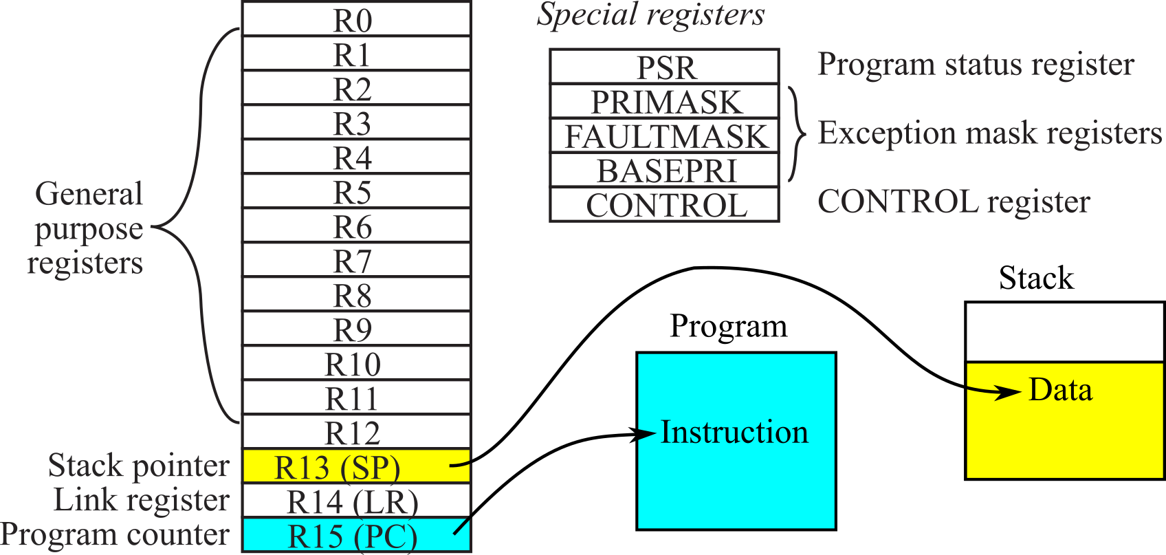
Figure 1.6.1. Registers on the ARM ® Cortex-M processor.
Checkpoint 1.7.1 : Where in memory should you put the stack? I.e., does the SP point to RAM or ROM?
Checkpoint 1.7.2 : Where in memory should you put the program? I.e., does the PC point to RAM or ROM?
The ARM Architecture Procedure Call Standard, AAPCS, part of the ARM Application Binary Interface (ABI), uses registers R0, R1, R2, and R3 to pass input parameters into a C function. Also according to AAPCS we place the return parameter in Register R0.
There are three status registers named Application Program Status Register (APSR), the Interrupt Program Status Register (IPSR), and the Execution Program Status Register (EPSR) as shown in Figure 1.7.2. These registers can be accessed individually or in combination as the Program Status Register (PSR). The N, Z, V, and C bits give information about the result of a previous ALU operation. In general, the N bit is set after an arithmetical or logical operation signifying whether or not the result is negative. Similarly, the Z bit is set if the result is zero. The C bit means carry and is set on an unsigned overflow, and the V bit signifies signed overflow.

Figure 1.7.2. The program status register of the ARM ® Cortex-M processor.
The T bit will always be 1, indicating the ARM ® Cortex ™ -M processor is executing Thumb ® instructions. The ISR_NUMBER indicates which interrupt if any the processor is handling. Bit 0 of the special register PRIMASK is the interrupt mask bit. If this bit is 1, most interrupts and exceptions are not allowed. If the bit is 0, then interrupts are allowed. There are four levels of interrupt priority. The BASEPRI register defines the priority of the executing software. It prevents interrupts with lower or equal priority but allows higher priority interrupts. For example if BASEPRI equals 2, then requests with level 0 and 1 can interrupt, while requests at levels 2 or 3 will be postponed. A lower number means a higher priority interrupt. The details of interrupt processing will be presented in Chapter 5.
Assembly language instructions have four fields separated by spaces or tabs. The label field is optional and starts in the first column and is used to identify the position in memory of the current instruction. You must choose a unique name for each label. The opcode field specifies the processor command to execute. The operand field specifies where to find the data to execute the instruction. Thumb instructions have 0, 1, 2, 3, or 4 operands, separated by commas. The comment field is also optional and is ignored by the assembler, but it allows you to describe the software making it easier to understand. You can add optional spaces between operands in the operand field. However, a // must separate the operand and comment fields. Good programmers add comments to explain the software.
Label Opcode Operands Comment
Func: MOVS R0, #100 // 100 means maximum
BX LR
Observation: A good comment explains why an operation is being performed, how it is used, how it can be changed, or how it was debugged. A bad comment explains what the operation does. The comments in the above two assembly lines are examples of bad comments.
The assembly source code is a text file (with Windows file extension .s) containing a list of instructions. The assembler translates assembly source code into object code, which are the machine instructions executed by the processor. All object code is halfword-aligned. This means instructions can be 16 or 32 bits wide, and the program counter bit 0 will always be 0. The listing is a text file containing a mixture of the object code generated by the assembler together with our original source code.
Label Opcode Operand comment
Func: MOVS R1,#0x64 // R1=100
MULS R0,R0,R1 // R0=100*input
ADDS R0,R0,#10 // R0=100*input+10
BX LR // return 100*input+10
When we build a project all files are assembled or compiled then linked together. The linker decides exactly where in memory everything will be. After building the project, it can be downloaded, which programs the object code into flash ROM. You are allowed to load and execute software out of RAM. But for an embedded system, we typically place executable instructions into nonvolatile ROM. The map file shows where in memory your variables and instructions exist.
The first action we present is bringing a constant value into a register. With immediate addressing mode, the data itself is contained in the instruction. Once the instruction is fetched no additional memory access cycles are required to get the data. Notice the number 100 (0x64) is embedded in the machine code of the MOVS instruction shown in Figure 1.6.3.
MOVS R0,#100 // R0=100, immediate addressing
Figure 1.7.3. An example of immediate addressing mode, data is in the instruction.
The constant value allowed by MOVS is limited to 8-bit values. On the other hand, the LDR instruction can be used to bring any 32-bit value into a register. Notice the number 0x12345678 is not embedded in the machine code of the instruction, but rather stored in ROM a short distance away, as shown in Figure 1.7.4. The assembler automatically places the constant in ROM and calculates the appropriate PC-relative offset. At the time of execution, the PC is pointing to the next instruction.
LDR R0,=0x12345678 // R0=0x12345678, PC-relative addressing
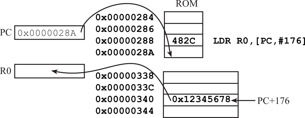
Figure 1.7.4. An example of using the LDR instruction to load any constant into a register.
A fundamental issue in program development is the differentiation between data and address. When we put the number 100 into Register R0, whether this is data or address depends on how the 100 is used. As presented in Program 1.6.1, we created a 32-bit global variable called Stuff. To write an initial value of 100 into this variable will take three instructions. In this example, R0 has data and R1 had an address. First, the MOVS instruction brings the desired value into R0. Second, the LDR instruction sets R1 to point to the global variable Stuff. Lastly, the STR instruction writes the value into the variable.
MOVS R0,#100
LDR R1,=Stuff // R1 points to the variable Stuff
STR R0,[R1] // Stuff=100
Figure 1.7.5. It takes three instructions to write to a global variable.
Checkpoint 1.7.3 : How would you modify the above assembly code to write 0x0E to Port A output?
To read the value of a variable into a register will take two instructions. After executing these two instructions, R3 will have a copy of the value from the global Stuff. The first LDR instruction sets R2 to point to the global variable Stuff. The second LDR instruction will read the value from the variable.
LDR R2,=Stuff // R2 points to the variable Stuff
LDR R3,[R2] // R3=Stuff
Figure 1.7.6. It takes two instructions to read from a global variable.
Checkpoint 1.7.4 : How would you modify the above assembly code to read from Port A input?
An aligned access is an operation where a word-aligned address is used for a word, dual word, or multiple word access, or where a halfword-aligned address is used for a halfword access. Byte accesses are always aligned. The address of an aligned word access will have its bottom two bits equal to zero. An unaligned word access means we are accessing a 32-bit object (4 bytes) but the address is not evenly divisible by 4. The following instructions support 32-bit memory access:
LDR Load 32-bit word
STR Store 32-bit word
Observation: 32-bit accesses using LDR and STR must be to word-aligned addresses.
The address of an aligned halfword access will have its bottom bit equal to zero. An unaligned halfword access means we are accessing a 16-bit object (2 bytes) but the address is not evenly divisible by 2. The following instructions support 16-bit memory access:
LDRH Load 16-bit unsigned halfword
LDRSH Load 16-bit signed halfword (sign extend bit 15 to bits 31-16)
STRH Store 16-bit halfword
Observation: 16-bit accesses using LDRH LSRSH and STRH must be to halfword-aligned addresses.
Transfers of one byte are allowed for the following instructions:
LDRB Load 8-bit unsigned byte
LDRSB Load 8-bit signed byte (sign extend bit 7 to bits 31-8)
STRB Store 8-bit byte
When loading a 32-bit register with an 8- or 16-bit value, it is important to use the proper load, depending on whether the number being loaded is signed or unsigned. This determines what is loaded into the most significant bits of the register to ensure that the number keeps the same value when it is promoted to 32 bits. When loading an 8-bit unsigned number, the top 24 bits of the register will become zero. When loading an 8-bit signed number, the top 24 bits of the register will match bit 7 of the memory data (signed extend). Note that there is no such thing as a signed or unsigned store. For example, there is no STRSH ; there is only STRH . This is because 8, 16, or all 32 bits of the register are stored to an 8-, 16-, or 32-bit location, respectively. No promotion occurs. This means that the value stored to memory can be different from the value located in the register if there is overflow. When using STRB to store an 8-bit number, be sure that the number in the register is 8 bits or less.
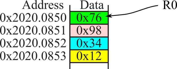
Figure 1.7.6. Assume these memory contents for Checkpoints 1.7.5 through 1.7.9.
Checkpoint 1.7.5 : Assume R0 equals 0x20200850 at the time LDR R1,[R0] is executed. To what value will R1 become?
Checkpoint 1.7.6 : Assume R0 equals 0x20200850 at the time LDRH R2,[R0] is executed. To what value will R2 become?
Checkpoint 1.7.7 : Assume R2 equals 0 and R0 equals 0x20200850 at the time LDRSH R3,[R0,R2] is executed. To what value will R3 become?
Checkpoint 1.7.8 : Assume R0 equal 0x20200850 at the time LDRB R4,[R0] is executed. To what value will R4 become?
Checkpoint 1.7.9 : Assume R2 equals 0 and R0 equals 0x20200850 at the time LDRSB R5,[R0,R2] is executed. To what value will R5 become?
Boolean Logic has two states: true (1) and false (0). A binary operation produces a single result given two inputs. The logical and (&) operation yields a true result if both input parameters are true. The logical or (|) operation yields a true result if either input parameter is true. The exclusive or (^) operation yields a true result if exactly one input parameter is true. The logical operators are summarized in the table below. The logical instructions on the ARM Cortex-M processor take two inputs, one from a register and the other either from a register or from a constant. These operations are performed in a bit-wise fashion on two 32-bit input parameters yielding one 32-bit output result. The result is stored into the destination register. For example, the calculation r=m&n means each bit is calculated separately, r31=m31&n31, r30=m30&n30. r0=m0&n0.
In C, when we write logical operations as r=m&n; r=m|n; r=m^n; the logical operation occurs in a bit-wise fashion also described by the table below. However, in C, we define the Boolean functions as r=m&&n; r=m||n; For Booleans, the operation occurs in a word-wise fashion. For example, r=m&&n; means r will become zero if either m is zero or n is zero. Conversely, r will become 1 (any nonzero) if both m is nonzero and n is nonzero.
| A | B | A&B | A|B | A^B | A&(~B) |
| Rn | Op2 | AND | ORR | EOR | BIC |
| 0 | 0 | 0 | 0 | 0 | 0 |
| 0 | 1 | 0 | 1 | 1 | 0 |
| 1 | 0 | 0 | 1 | 1 | 1 |
| 1 | 1 | 1 | 1 | 0 | 0 |
Table 1.7.1. Logical operations performed by the Cortex-M processor.
All instructions place the result into the destination register Rd. If Rd is omitted, the result is placed into Rn, which is the register holding the first operand. The N and Z condition code bits are updated on the result of the operation. The second operand is a register. We use the ANDS instruction to mask or select bits. We use the ORRS instruction to set bits. We use the EORSinstruction to toggle bits (change from 0 to 1 or 1 to 0) bits. We use the BICS instruction to clear bits.
ANDS Rd, Rn, Rm // Rd=Rn&Rm
ORRS Rd, Rn, Rm // Rd=Rn|Rm
EORS Rd, Rn, Rm // Rd=Rn^Rm
BICS Rd, Rn, Rm // Rd=Rn&(~Rm)
Assume Port B bit 1 (PB1) is an output. The following example sets the PB1 pin high. Notice that this code will leave the other pins unchanged.
// C version
GPIOB->DOUT31_0 = GPIOB->DOUT31_0 | 0x02;
// assembly version
LDR R0,=GPIOB_DOUT31_0 // pointer to output register
LDR R1,[R0] // previous values
MOVS R2,#0x02 // mask for bit 1
ORRS R1,R1,R2 // set bit 1
STR R0,[R1] // change actual output
Again, assume Port B bit 1 (PB1) is an output. The following example clears the PB1 pin low, without changing any other pins.
// C version
GPIOB->DOUT31_0 = GPIOB->DOUT31_0 & ~0x02;
// assembly version
LDR R0,=GPIOB_DOUT31_0 // pointer to data register
LDR R1,[R0] // previous values
MOVS R2,#0x02 // mask for bit 1
BICS R1,R1,R2 // clear bit 1
STR R0,[R1] // change actual output
Checkpoint 1.7.10 : How would you change the above program to set the PB3 pin?
Checkpoint 1.7.11 : How would you change the above program to toggle the PB2 pin?
Like programming in C, the assembly shift instructions take two input parameters and yield one output result. In C, the left shift operator is >. E.g., to left shift the value in m by n bits and store the result in r we execute: r = m. Similarly, to right shift the value in m by n bits and store result r, we execute: r=m>>n.
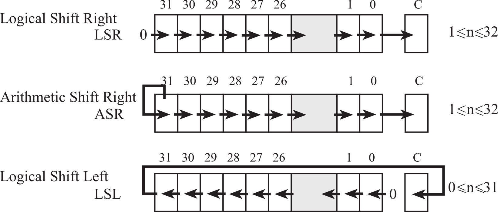
Figure 1.7.7. Shift operations move bits to the right or left.
The logical shift right (LSRS) is similar to an unsigned divide by 2 n , where n is the number of bits shifted. A zero is shifted into the most significant position, and the carry flag will hold the last bit shifted out. The right shift operations do not round. For example, a right shift by 3 bits is similar to divide by 8. However, 15 right-shifted three times (15>>3) is 1, while 15/8 is much closer to 2. In general, the LSR discards bits shifted out.
The arithmetic shift right (ASRS) is similar to a signed divide by 2 n . Notice that the sign bit is preserved, and the carry flag will hold the last bit shifted out. This right shift operation also does not round. Again, a right shift by 3 bits is similar to divide by 8. However, -9 right-shifted three times (-9>>3) is -2, while implementing -9 divided by 8 using the SDIV instruction yields -1. In general, the ASR discards bits shifted out, and the SDIV truncates towards 0.
The logical shift left (LSLS) operation works for both unsigned and signed multiply by 2 n . A zero is shifted into the least significant position, and the carry bit will contain the last bit that was shifted out.
All shift instructions place the result into the destination register Rd. Rm is the register holding the value to be shifted. The number of bits to shift is either in register Rs, or specified as a constant n. The N and Z condition code bits are updated on the result of the operation. The C bit is the carry out after the shift. These shift instructions will leave the V bit unchanged.
Observation: Use logic shift for unsigned numbers and arithmetic shifts for signed numbers.
LSRS Rd, Rm, Rs // logical shift right Rd=Rm>>Rs (unsigned)
LSRS Rd, Rm, #n // logical shift right Rd=Rm>>n (unsigned)
ASRS Rd, Rm, Rs // arithmetic shift right Rd=Rm>>Rs (signed)
ASRS Rd, Rm, #n // arithmetic shift right Rd=Rm>>n (signed)
LSLS Rd, Rm, Rs // shift left Rd=Rm LSLS Rd, Rm, #n // shift left Rd=Rm
Checkpoint 1.7.12 : If R0=0xC0123456, what will be the value in R0 after LSRS R0,R0,#4 is executed?
Checkpoint 1.7.13 : If R0=0xC0123456, what will be the value in R0 after ASRS R0,R0,#4 is executed?
Checkpoint 1.7.14 : If R0=0xC0123456, what will be the value in R0 after LSLS R0,R0,#4 is executed?
When software executes arithmetic instructions, the operations are performed by digital hardware inside the processor. Even though the design of such logic is complex, we will present a brief introduction, in order to provide a little insight as to how the computer performs arithmetic. It is important to remember that arithmetic operations (addition, subtraction, multiplication, and division) have constraints when performed with finite precision on a processor. An overflow error occurs when the result of an arithmetic operation cannot fit into the finite precision of the register into which the result is to be stored. The N C V and Z condition code bits are updated on the result of the operation.
The immediate value #n can be any 8-bit unsigned constant. When Rd is absent, the result is placed back in Rn.
ADDS Rd, Rn, Rm // Rd = Rn + Rm
ADDS Rd, Rn, #n // Rd = Rn + n
SUBS Rd, Rn, Rm // Rd = Rn - Rm
SUBS Rd, Rn, #n // Rd = Rn - n
CMP Rn, Rm // Rn - Rm
CMP Rn, #n // Rn - n
The compare instruction CMP does not save the result of the subtraction but always sets the condition code. The compare instructions are used to create conditional execution, such as if-then, for loops, and while loops.
The addition and subtraction instructions set the condition code bits as shown in the following table. The addition and subtraction instructions work for both signed and unsigned values. As designers, we must know in advance whether we have signed or unsigned numbers. The computer cannot tell from the binary which type it is, so it sets both C and V. Our job as programmers is to look at the C bit if the values are unsigned and look at the V bit if the values are signed.
| Bit | Name | Meaning after addition or subtraction |
| N | Negative | Result is negative |
| Z | Zero | Result is zero |
| V | Overflow | Signed overflow |
| C | Carry | Unsigned overflow |
Table 1.7.2. Condition code bits contain the status of the previous arithmetic operation.
Observation: The carry bit, C, is set after an unsigned addition when the result is incorrect. The carry bit, C, is cleared after an unsigned subtraction when the result is incorrect.
Observation: The overflow bit, V, is set after a signed addition or subtraction when the result is incorrect.
To understand the multiplication algorithm, consider these two assembly functions that multiply two 8-bit unsigned integers, A and B, yielding a 16-bit result, R. In general, an n-bit number multiplied by an m-bit number yields an (n+m)-bit product. The slow algorithm, initializes R=0, and then adds R=R+A, B times. The slow algorithm is simple to understand, but very slow. In particular, if B is 255, then this algorithm requires 4*255+3=1023 instructions to complete. The fast algorithm is designed with the basis elements of a binary number in mind. If bit n of A is set, then R=R+2 n *B. We initialize a loop counter at 8 because the multiplier is 8 bits, the product is initially 0. The LSRS instruction shifts the least significant bit into the carry, deciding whether or not the multiplier needs to be added. Each time through the loop the multiplier is shifted right and multiplicand is shifted left. This fast algorithm takes to 44 to 52 instructions to complete.
| // Inputs: A=R0 is 8-bit unsigned // B=R1 is 8-bit unsigned // Output: R=A*B is 16-bit product slowmul: MOVS R2,#0 // R2 is result R loop: CMP R1,#0 // quit when B=0 BEQ done ADDS R2,R2,R0 // R=R+A B loop done: MOVS R0,R2 // result in R0 BX LR | // Inputs: A=R0 is 8-bit unsigned // B=R1 is 8-bit unsigned // Output: R=A*B is 16-bit product fastmul: MOVS R2,#8 // loop counter MOVS R3,#0 // product loop: LSRS R0,R0,#1 // check next bit in multiplier BCC next // skip if bit is 0 ADDS R3,R1 // add multiplicand next: LSLS R1,R1,#1 // next bit is twice the value SUBS R2,R2,#1 BNE loop MOVS R0,R3 // product BX LR |
Program 1.7.1. Two multiply algorithms.
Next, let's convert Program 1.7.1 to multiply two 16-bit unsigned integers. The same code on the left operates for any size inputs up to 32 bits (neither algorithm checks for overflow). To change the code on the right to 16 by 16, we simply change the loop counter to 16. If B is 65535, then the left algorithm requires 4*65535+3=262140 instructions to complete (256 times slower). However, for the fast algorithm, because the loop counter is doubled, it only runs twice as slow.
Multiply (MULS) uses 32-bit operands and produces a 32-bit result. This multiply instruction only saves the bottom 32 bits of the result. They can be used for either signed or unsigned numbers, but no overflow flags are generated. If the Rd register is omitted, the Rn register is the destination. The MULS does set the Z and N bits are set according to the result.
MULS Rd, Rd, Rm // Rd = Rd * Rm
Checkpoint 1.7.15 : If one adds an n-bit number to another n-bit number, how total bits are in the sum?
Checkpoint 1.7.16 : If one multiplies an n-bit number to an m-bit number, how total bits are in the product?
The Cortex M0+ does not have a division instruction. So, to divide we will need to implement the operation as a function. Consider these two assembly functions that divide a 32-bit unsigned dividend, A by a 16-bit unsigned divisor, B, yielding a 16-bit quotient, Q and a 16-bit remainder R. Notice that both these algorithms return two values (R0, R1), and therefore are not AAPCS compliant. The definition of unsigned divide is
A = Q*B+R assuming RB
The slow algorithm counts how many times we can subtract the divisor from the dividend. It is easy to understand, but very slow. If the dividend is 65535 and the divisor is 1, the slow algorithm requires 65535*5+4=327679 instructions to execute. The fast algorithm is designed with the basis elements of a binary number in mind, modeled after we perform long division. We left shift the divisor under the dividend as many times as we can while the shifted divisor is less than the dividend. When then set the bit in the quotient and subtract the shifted divisor from the dividend. The fast algorithm takes to from 105 to 127 instructions to complete.
| // Inputs: A=R0 is 32-bit unsigned dividend // B=R1 is 16-bit unsigned divisor // Outputs: Q=A/B is 16-bit quotient // B=R1 is 16-bit remainder slowdiv: // R0 becomes the remainder, R MOVS R2,#0 // R2 is quotient Q loop: CMP R0,R1 // quit when R BLO done ADDS R2,R2,#1 // Q=Q+1 SUBS R0,R0,R1 // A=A-B B loop done: MOVS R1,R0 // remainder in R1 MOVS R0,R2 // quotient in R0 BX LR | // Inputs: A=R0 is 32-bit unsigned dividend // B=R1 is 16-bit unsigned divisor // Outputs: Q=A/B is 16-bit quotient // B=R1 is 16-bit remainder fastdiv: PUSH LDR R4,=0x00010000 // bit mask MOVS R3,#0 // quotient MOVS R2,#16 // loop counter LSLS R1,#15 // move divisor under dividend loop: LSRS R4,R4,#1 // bit mask 15 to 0 CMP R0,R1 // need to subtract? BLO next SUBS R0,R0,R1 // subtract divisor ORRS R3,R3,R4 // set bit next: LSRS R1,R1,#1 SUBS R2,R2,#1 BNE loop MOVS R1,R0 // remainder MOVS R0,R3 // quotient POP |
Program 1.7.2. Two divide algorithms.
Observation: You will use the fast divide algorithm in Lab 6 to convert an integer into a sequence of ASCII characters by dividing the integer by 10, and using both the quotient and remainder.
In this course we will construct software using only three basic building blocks: sequence, conditional, and loop, see Figure 1.8.1. We will use the conditional branch instructions to create this software block.
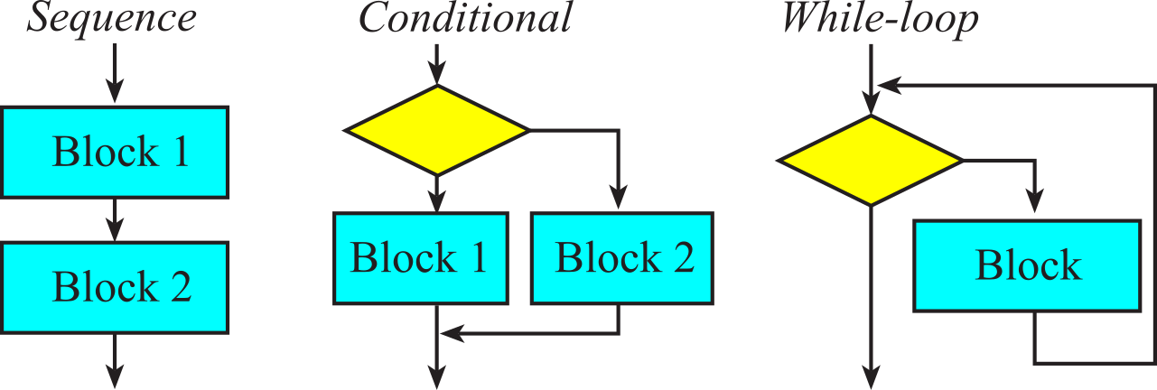
Figure 1.8.1. Structured programming uses these three basic structures.
Normally the computer executes one instruction after another in a linear fashion, which constitutes the sequence. In particular, the next instruction to execute is found immediately following the current instruction. We use branch instructions to deviate from this straight line path, creating the conditional and the loop. The following lists a few of the many branch instructions. The conditional branching must be preceded by an instruction that sets the condition code bits.
B label // unconditional branch to label
BEQ label // branch to label if Z=1
BNE label // branch to label if Z=0
BMI label // branch to label if N=1
BPL label // branch to label if N=0
BCS label // branch to label if C=1
BCC label // branch to label if C=0
BVS label // branch to label if V=1
BVC label // branch to label if V=0
One of the ways we affect execution flow is the conditional. To compare two values, they must be the same type.
First, we present an approach to conditionally test for individual bits. Let mask specify which bit to test. For example, to test bit 3, we set the mask to 0x08. In general the mask for bit n is 1. The approach is
Bring the entire value into R0
Bring the 1 mask value into R1
Check for bit n using ANDS R0,R0,R1
Execute one of the following conditionals
BEQ target // Branch if R0 bit n is 0
BNE target // Branch if R0 bit n is 1
To illustrate the conditional, let's write software that sets bit 1 of variable V1 to 1 if bit 8 of variable V0 is set, see Figure 1.8.2 and Program 1.8.1. Notice, we skip over the body if bit 8 is clear.
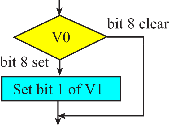
Figure 1.8.2. Flowchart of a conditional statement.
For the assembly implementation, we assume variable V0 is in register R0 and V1 is in register R1. The mask for bit 8 is 0x0100. The assembly version destroys R2 R3.
LDR R2,=0x0100
ANDS R2,R2,R0
MOVS R2,#0x02 // mask for set bit 1
ORRS R1,R1,R2 // set bit 1
if((V0&0x0100) == 0x0100
Program 1.8.1. Conditional to test individual bits.
To illustrate the loop, we will implement a simple unsigned multiply, see Figure 1.8.3 and Program 1.8.2. We assume R0(n0) and R1(n1) are the inputs and function will perform R0*R1, placing the product in R2(n2). We initialize a sum in R2, which will be converted to the product. In a while-loop the ending condition is tested before the loop statement. This is necessary because R1 might be 0, meaning the loop statement should never be executed. During each loop statement, R0 is added to R2, and R1 is decremented.
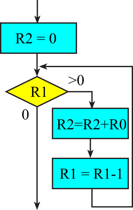
Figure 1.8.3. Flowchart of a conditional statement.
MOVS R2,#0 // sum
loop: CMP R1,#0 // is n1 equal 0?
BEQ done
ADDS R2,R2,R0 // sum = sum+n0
SUBS R1,R1,#1 // n1 = n1-1
B loop // n1 = n1-1
done:
sum = 0;
while(n1) sum = sum+n0;
n1 = n1-1;
>
Program 1.8.2. While-loop to implement multiply.
Next, we present if-then for signed 32-bit integers. The approach is
Bring the first value into R0
Bring the second value into R1
Compare the two values using CMP R0,R1
Execute one of the following signed conditionals
BEQ target // Branch if R0 equals R1
BNE target // Branch if R0 does not equal R1
BLT target // Branch if R0 is less than R1 (signed)
BLE target // Branch if R0 is less than or equal to R1 (signed)
BGE target // Branch if R0 is greater than or equal to R1 (signed)
BGT target // Branch if R0 is greater than R1 (signed)
The approach is similar when comparing two unsigned 32-bit integers
Bring the first value into R0
Bring the second value into R1
Compare the two values using CMP R0,R1
Execute one of the following unsigned conditionals
BEQ target // Branch if R0 equals R1
BNE target // Branch if R0 does not equal R1
BLO target // Branch if R0 is less than R1 (unsigned)
BLS target // Branch if R0 is less than or equal to R1 (unsigned)
BHS target // Branch if R0 is greater than or equal to R1 (unsigned)
BHI target // Branch if R0 is greater than R1 (unsigned)
As our software becoming more complex, we will need to create functions. The SP points to data on the top of the stack. We use push to save data and pop to retrieve data. The stack operates in a last in first out manner. Let's present rules for using the stack
1. Functions should have an equal number of pushes and pops
2. Stack accesses should not be performed outside the allocated area
3. Stack reads and writes should not be performed within the free area
4. Stack push should first decrement SP, then store the data
5. Stack pop should first read the data, and then increment
The stack grows downwards in memory as we push data on to it so, although we refer to the most recent item as the “top of the stack” it is actually the item stored at the lowest address! To push data on the stack, the stack pointer is first decremented by 4, and then the 32-bit information is stored at the address specified by SP. To pop data from the stack, the 32-bit information pointed to by SP is first retrieved, and then the stack pointer is incremented by 4. SP points to the last item pushed, which will also be the next item to be popped. The boxes in Figure 1.9.1 represent 32-bit storage elements in RAM. The grey boxes in the figure refer to actual data stored on the stack, and the white boxes refer to locations in the stack area, but do not contain stack data. This figure illustrates how the stack is used to push the contents of Registers R0, R1, and R2 in that order. Assume Register R0 initially contains the value 1, R1 contains 2, and R2 contains 3. The drawing on the left shows the initial stack. The software executes these six instructions in this order:

Figure 1.9.1. Stack picture showing three numbers first being pushed, then three numbers being popped. You are allowed to draw stack pictures so that the lowest address is on the top (like this one) or so that lowest address is on the bottom. It is important however to be clear, accurate, and consistent.
Remember the order in the register list does not matter. The register with the lower number is stored in memory with the lower address. These are the same instructions
We use the BL instruction to call a subroutine. The BL instruction will save the return address in LR and branch to the subroutine. The BX LR will return the LR back into the PC, causing control flow to revert back to the place from which the function was called. If one function calls another it will need to save the LR on the stack. In general we will adhere to the following rules according to ARM Architecture Procedure Call Standard (AAPCS)
We use R0,R1,R2,R3 as input parameters
We use R0 as the return parameter.
We can freely use R0,R1,R2,R3,R12 without needing to push or pop.
We can use R4-R11, but must push the values at the start and pop the values at then end.
There are two aspects of a function in assembly. First the aspect is the definition. The first three lines of Program 1.9.1 are comments, which explain what the function does. The explanation describes the input parameters and output parameter. Line 4 creates an assembly label specifying the entry point of the function. In this example, lines 5 and 6 perform the body of the function. Comments inside the body should explain how the function works. Line 7 is the function return using the BX LR instruction. Figure 1.9.2 shows the flowchart syntax for a function
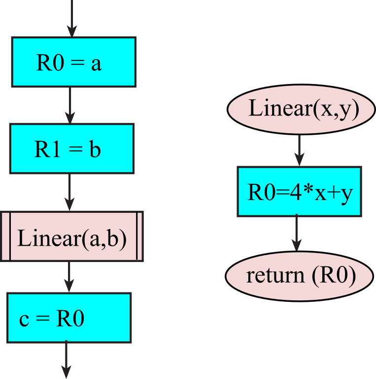
Figure 1.9.2. Flowchart of a function; left is function invocation, right is the function definition.
// Inputs: x in R0 1
// y in R1 2
// Outputs: z = 4*x+y in R0 3
Linear: // 4
LSLS R0,#2 // R0=4*x 5
ADDS R0,R0,R1 // R0=4*x+y 6
BX LR // return 7
Program 1.9.1. Function definition in assembly.
Second the aspect is the invocation. Before we invoke a function, we establish the input parameters. Assume a,b,c are global variables. Lines 8-11 set the input parameters R0 to a and R1 to b. Line 12 is the invocation using the BL instruction. After the function returns, we process the output result. In this case, the result is stored in c. The overall effect is to implement c=4*a+b
LDR R0,=a // 8
LDR R0,[R0] // R0 is a 9
LDR R1,=b // 10
LDR R1,[R1] // R1 is b 11
BL Linear // invocation 12
LDR R1,=c // 13
STR R0,[R1] // c = 4*a+b 14
Program 1.9.2. Function invocation in assembly.
Checkpoint 1.9.1 : What happens to the LR when the BL instruction is executed?
Checkpoint 1.9.2 : How does the BX LR instruction return from the function?
Checkpoint 1.9.3 : What must you do if one function calls another function?
A struct is a object with containing multiple fields having different types. A list contains multiple structs. In Figure 1.10.1, each struct has three fields: an ID, an Exam1 and an Exam2. The first field is a 32-bit ID. The second and third fields are 16-bit grades. E.g., the student with ID=7 has an Exam1 of 96 and an Exam2 of 82. Because each struct is 8 bytes, they can be stored contiguously. The end of the list is signified by a ID value of -1, called a sentinel. Program 1.10.1 defines this list in ROM. The function ID2Exam1 takes an ID and looks up their Exam1. If R1 points to a struct, then [R1,#0] accesses the ID, [R1,#4] accesses Exam1, and [R1,#6] accesses Exam2. Notice in assembly, to change the pointer to the next struct we add 8. In C, we add 1, and the compiler creates code that actually adds 8.

Figure 1.10.1. A list is an array of structs. Each struct has multiple elements with different types.
.text
.align 2
List: .long 5 // ID
.short 95,96 // Scores
n1: .long 7
.short 96,82
n2: .long 2
.short 94,99
n3: .long 1
.short 95,86
n4: .long -1 // sentinel
.short 0,0 // NA
ID2Exam1: // R0 is the ID
LDR R1,=List // pointer
LDR R3,=-1 // sentinel
look: LDR R2,[R1,#0] // ID
CMP R2,R3
BEQ fail // end?
CMP R2,R0
BEQ yes // found
ADDS R1,R1,#8 // next
B look
fail: MOVS R0,#0 // fail
B done
yes: LDRH R0,[R1,#4] // Exam1
done: BX LR
Program 1.10.1. A list with four structs stored in ROM, the fifth struct is the sentinel.